Instrumentation
Use cutting-edge equipment
Conduct your research with our high-end technology.
All listed instruments are available for rent by the hour.
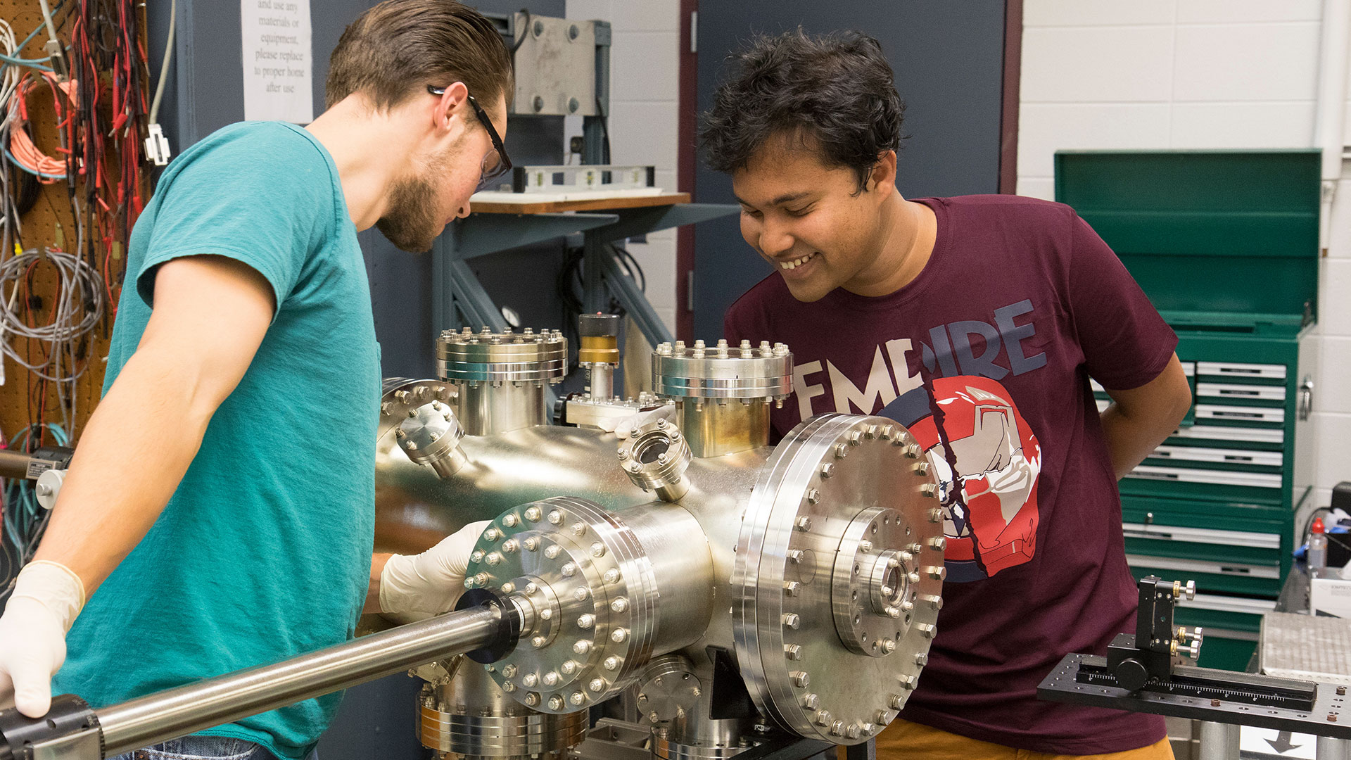
Browse our tools
Locate the equipment you need and request a reservation to use it.
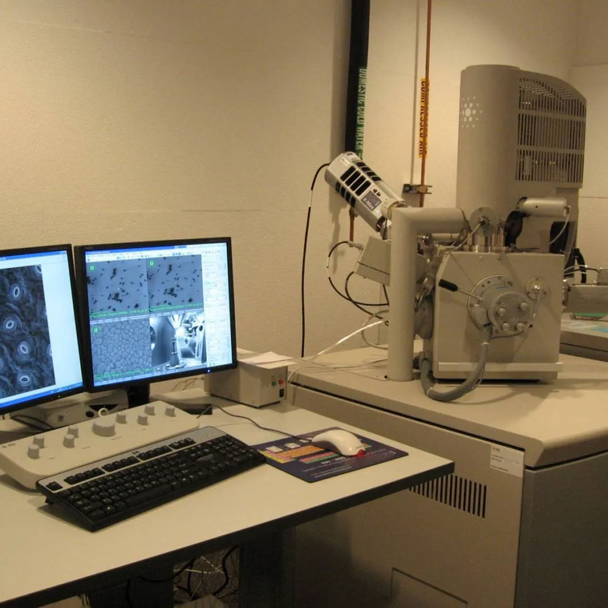
- FESEM: Field-Emission Scanning Electron Microscope
- FT-IR: Fourier Transform Infrared Spectrometer
- PLD: Pulsed Laser Deposition
- Raman Spectrometer
- RF Sputter Deposition
- SQUID: Superconducting Quantum Interference Device Magnetometer
- UV-Vis: Ultraviolet-visible Spectroscopic Microscopic
- X-ray Diffraction
FESEM: Field-Emission Scanning Electron Microscope
- Explores correlations between morphology, structures and compositions of various nanomaterials and their electrical, optical, magnetic and biology properties.
- Provides high resolution secondary electron and backscattered electron images of surface topography, spatial elemental distribution and internal structures for materials.
Located in Kemper Hall 101A. Contact Dr. David Cornelison to make a reservation.
FT-IR: Fourier Transform Infrared Spectrometer
- Used to acquire near infrared to far infrared spectra
- Measures with an interferometer to collect and digitize an interferogram.
Located in Kemper Hall 101A. Contact Dr. David Cornelison to make a reservation.
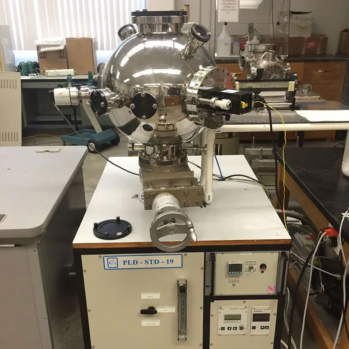
PLD: Pulsed Laser Deposition
- Used to prepare high quality thin films of high Tc oxides, ferroelectrics, high dielectrics, semiconductors, polymers, metals and alloys for applications in electric, magnetic and optical devices.
- Unique performance and versitility in materials science.
Located in Kemper Hall 103G. Contact Dr. Kartik Ghosh to make a reservation.
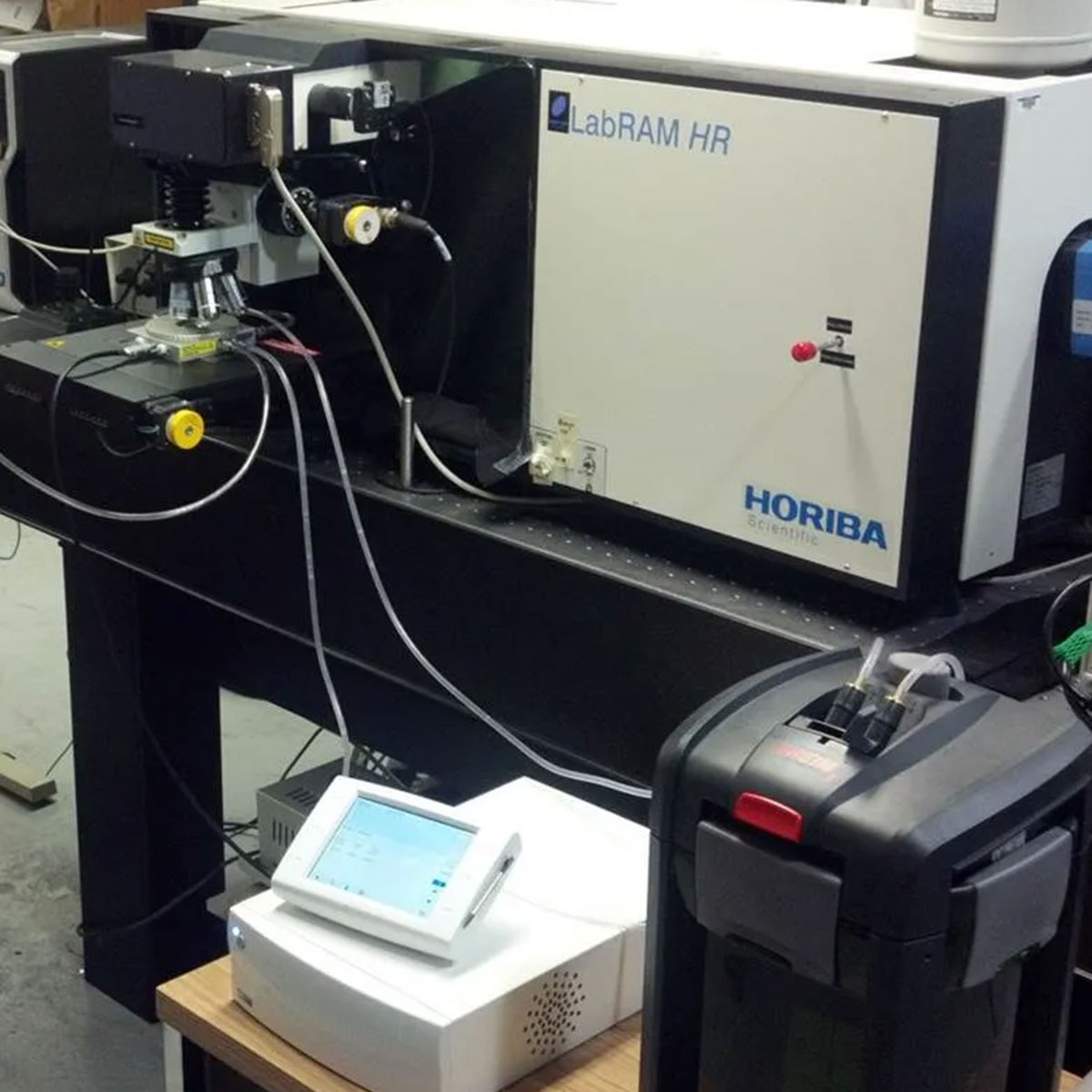
Raman Spectrometer
- A spectroscopic technique based on inelastic scattering of monochromatic light, usually from a laser source.
- Used to study solid, liquid and gaseous samples.
- Provides direct information on the vibrational characteristics of the sample.
Located in Kemper Hall 101E. Contact Dr. Robert Mayanovic to make a reservation.
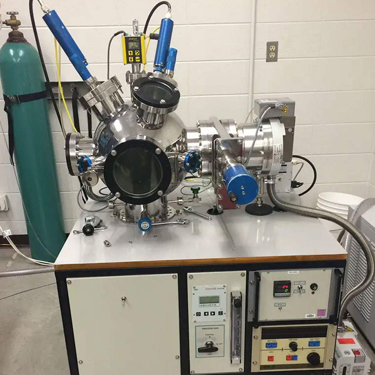
RF Sputter Deposition
- A physical vapor deposition (PVD) method of thin film deposition by sputtering. Material is ejected from a target (source) onto a substrate.
- Grows high quality thin films of various metals, insulators and semiconductors.
- Prepares high quality electrodes for various types of electronic devices.
Located in Kemper Hall 103G. Contact Dr. Kartik Ghosh to make a reservation.
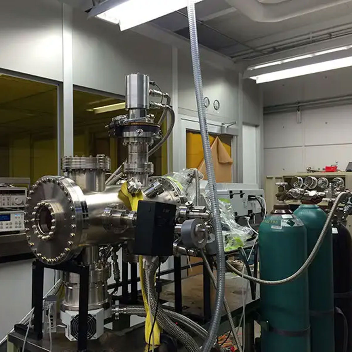
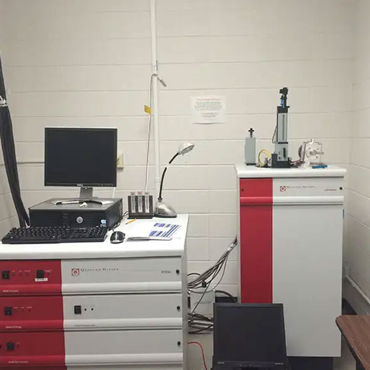
SQUID: Superconducting Quantum Interference Device Magnetometer
- Used to measure extremely subtle magnetic fieldbased on superconducting loops containing Josephson junctions.
- Provides solutions for a unique class of sensitive magnetic measurements in areas like high-temperature superconductivity, biochemistry and magnetic recording media.
- Studies AC/DC magentization magnetoresistance, and Hall effect of magnetic and electronic materials.
Located in Kemper Hall 103G. Contact Dr. Kartik Ghosh to make a reservation.
UV-Vis: Ultraviolet-visible Spectroscopic Microscope
- Absorbs spectroscopy or reflectance spectroscopy in the ultraviolet visible spectral region.
- Light is passed through a sample substance to determine its transmittance and reflectance.
Located in Kemper Hall 101A. Contact Dr. David Cornelison to make a reservation.
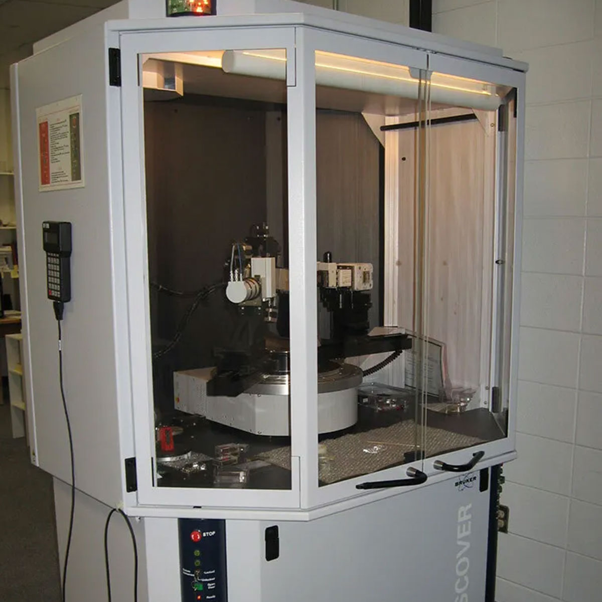
X-ray Diffraction
- Technique based on elastic scattering of x-rays from the atomic arrangement within a sample.
- Provides information on the structural atomic arrangement of a solid, powder or thin film sample.
Located in Kemper Hall 101E. Contact Dr. Robert Mayanovic to make a reservation.
Resources